Can ai defect detection map six atomic defects in semiconductors noninvasively?
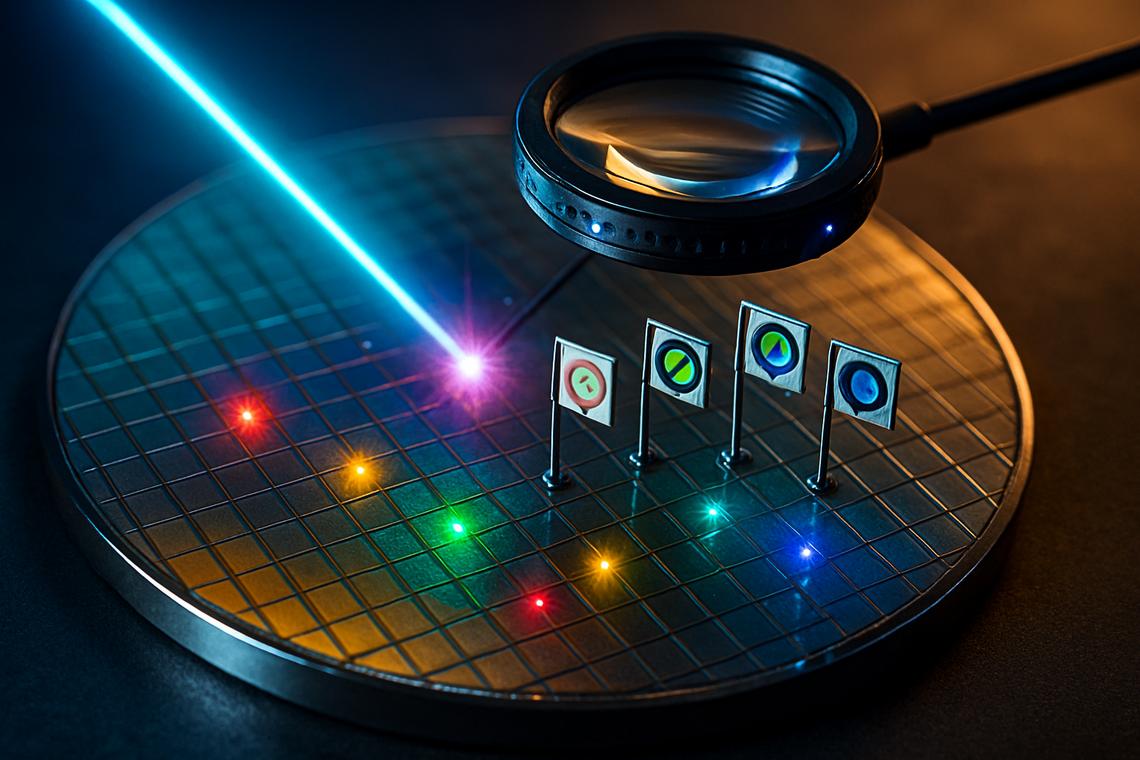
Researchers at MIT have developed a new approach that uses ai defect detection to identify tiny imperfections in materials without cutting or damaging the samples.
AI model targets atomic-scale defects
In materials science, microscopic flaws can be an asset rather than a liability, since deliberately engineered defects often enhance mechanical strength, heat transfer, or energy-conversion efficiency. However, accurately mapping these defects in finished products has long challenged engineers.
To address this problem, a team at MIT has built an AI model that classifies and quantifies atomic-scale defects using data from a noninvasive neutron-scattering technique. The system, trained on 2,000 different semiconductor materials, can simultaneously detect up to six kinds of point defects, something conventional approaches cannot achieve.
“Existing techniques can’t accurately characterize defects in a universal and quantitative way without destroying the material,” explains Mouyang Cheng, a PhD candidate in the Department of Materials Science and Engineering. Moreover, he notes that without machine learning, resolving six distinct defect types in one analysis “is unthinkable.”
The researchers argue that this capability marks a step toward much finer control of defects in products such as semiconductors, microelectronics, solar cells, and advanced battery materials. That said, they stress that complementary methods are still needed to see the “full elephant” of complex defect landscapes.
Limitations of conventional defect analysis
Manufacturers have become adept at deliberately introducing defects through techniques like doping, yet quantifying defect concentrations remains largely an exercise in estimation. “Engineers have many ways to introduce defects, like through doping, but they still struggle with basic questions like what kind of defect they’ve created and in what concentration,” says postdoc Chu-Liang Fu.
Unwanted defects, such as oxidation or impurities introduced during synthesis, further complicate the picture. However, each established method for probing defects has strict limits. X-ray diffraction and positron annihilation can only characterize specific defect types, while Raman spectroscopy can reveal defect categories but not their concentration directly.
Another widely used tool, the transmission electron microscope, requires cutting ultrathin slices of a sample for imaging. That makes it invasive and unsuitable for high-throughput quality control on finished parts. Consequently, many materials harbor multiple, poorly quantified defect populations that may degrade performance in ways manufacturers do not fully understand.
Training the model with neutron data
In earlier work, lead researcher Mingda Li and collaborators showed that machine learning applied to spectroscopy data could classify crystalline materials. For this study, the team expanded that strategy to focus specifically on defects and their concentrations.
The group constructed a computational database of 2,000 semiconductor materials, then generated sample pairs for each: one pristine, one doped to introduce specific defects. Using the same neutron-scattering technique for every pair, they measured the vibrational frequencies of atoms within the solid materials and compiled a rich dataset.
“That built a foundational model that covers 56 elements in the periodic table,” Cheng says. The network uses a multihead attention mechanism, the same architecture underlying tools like ChatGPT. Moreover, it learns to extract subtle differences in vibrational spectra between defect-free and doped samples, then predicts which dopants are present and at what concentrations.
After fine-tuning the system and validating it with experimental measurements, the researchers showed the model could accurately estimate defect concentrations in an alloy widely used in electronics, as well as in a distinct superconductor material. This demonstrated that the approach is not confined to a single compound.
Quantifying multiple point defects at once
To probe the limits of their framework, the scientists doped certain materials multiple times to introduce several kinds of point defects simultaneously. They then asked the model to recover both the types and relative amounts of these defects from neutron-vibration data alone.
The AI proved capable of predicting up to six different point defects within a single material, and it could resolve defect concentrations as low as 0.2 percent. However, this level of performance surprised even the team. “It’s very challenging to decode the mixed signals from two different types of defects — let alone six,” Cheng notes.
According to the researchers, this middle-ground experiment highlights how ai defect detection can distinguish overlapping spectral patterns that would appear nearly identical to human analysts. Moreover, the results point to a more systematic route toward what they call “defect-aware” materials engineering.
From lab method to industrial tool
In current semiconductor and microelectronic manufacturing, companies typically test only a small subset of finished products using invasive characterization. This workflow slows feedback and makes it difficult to spot every problematic defect, especially when multiple types coexist in complex ways.
“Right now, people largely estimate the quantities of defects in their materials,” says undergraduate researcher Bowen Yu. Checking those estimates requires multiple specialized techniques, each probing just a small region or single grain of the sample. As a result, Yu adds, manufacturers can easily misinterpret which defects are actually present and in what amounts.
The MIT team’s approach, based on neutrons and vibrational spectra, offers a more comprehensive picture, but it is not yet practical for most factories. “This method is very powerful, but its availability is limited,” notes master’s student Eunbi Rha. Moreover, she explains that while vibrational spectra are conceptually simple, experimental setups for neutron measurements can be complex and large-scale.
Because of that, Li and colleagues are exploring more accessible pathways. Companies already use Raman-based tools extensively for semiconductor defect detection, and several industrial partners have asked when a similar AI-driven model could work with Raman data instead of neutrons.
Toward broader, noninvasive defect mapping
Responding to this demand, the researchers plan to develop a Raman spectroscopy model that mirrors their neutron-based system but relies on the scattering of light rather than neutrons. In parallel, they aim to extend their framework beyond point defects to capture larger structural features such as grains and dislocations that also influence material performance.
For Yongqiang Cheng and Douglas L Abernathy PhD ’93 of Oak Ridge National Laboratory, who co-authored the paper, the work underscores how combining advanced spectroscopic tools with artificial intelligence can unlock new views of matter. However, they emphasize that experimental validation will remain essential as models expand.
Ultimately, the team sees their study as a proof of concept for deploying ai-powered defect detection across a range of measurement platforms. To the human eye, Li says, defect signals in vibrational spectra often look nearly identical. Yet AI pattern recognition can tease apart subtle variations and infer the true defect landscape with quantitative precision.
“Defects are this double-edged sword,” Li observes. “There are many good defects, but if there are too many, performance can degrade. This opens up a new paradigm in defect science.” The research, published in the journal Matter, received support from the Department of Energy and the National Science Foundation and builds on work dating back to 2021.
In summary, the MIT team has shown that AI, combined with neutron-scattering vibrational data, can map multiple atomic-scale defects at once, offering a powerful noninvasive route to more precisely engineered materials.
You May Also Like

Lovable AI’s Astonishing Rise: Anton Osika Reveals Startup Secrets at Bitcoin World Disrupt 2025

XRP Price Outlook For April 2026